Keyboard Controller Chips: Real Gaming Performance Impact
19th Mar•7 min read
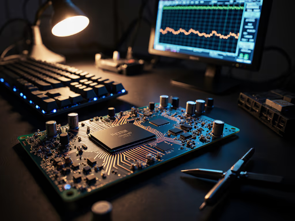
Keyboard PCB layout engineering sits underneath almost every "fast" board spec you see in marketing. Polling rate, debounce, and firmware matter, but the way the PCB is architected and routed quietly shapes real-world latency, stability, and comfort. When you approach pc gaming pcb design with both signal and hand mechanics in mind, you get a board that not only benchmarks well, but stays consistent through long sessions.
Your hands are part of the build.
Below is a FAQ-style deep dive aimed at gamers and hobbyists who want clear, practical answers (without needing a full electrical engineering degree).
Short version: PCB layout rarely changes latency by whole milliseconds, but it absolutely affects how predictably fast your board feels.
A typical wired mechanical gaming keyboard has:
The pure electrical delay along copper traces on a PCB is in nanoseconds... far below what you can feel. So why does keyboard pcb layout engineering matter at all?
Because layout drives:
A clean, well-thought layout lets firmware run aggressive scan and debounce settings with fewer safety margins. That's where perceptible wins show up: more responsive feeling keys without false triggers.
If you've ever used a "fast" spec board that occasionally double-pressed or dropped inputs under heavy RGB load, you've seen what happens when layout, firmware, and power design aren't aligned.
This is where trace design gaming impact becomes concrete.
Most gaming keyboards use a matrix:
In that setup, PCB choices matter:
In a good pc gaming pcb design, routing isn't just about making connections, it's about making the matrix predictable. That predictability is what lets firmware maintain an ultra-regular scan cadence, which you perceive as consistent response.
Think in terms of robustness more than raw speed. Clean routing lets the keyboard run "light-touch" filters and debounce, trimming effective latency.
Key guidelines:
These practices don't shave whole milliseconds on their own, but together they make signal routing gaming performance more deterministic. No mystery double-taps mid-fight, no intermittent disconnects when you slam multiple modifiers with RGB at full brightness. For firmware-side tuning of scan rate, debounce, and polling, see our gaming keyboard firmware guide.
At the USB speeds used by keyboards, pcb electromagnetic interference is usually more about reliability than raw speed.
Potential impacts:
Layout mitigations:
For a wired board, these steps are mostly about ensuring that your keyboard behaves the same way in a tournament venue (as it does at home near your router and monitor). That kind of stability is underrated, but it matters. If you're going wireless, compare Bluetooth vs 2.4GHz for gaming to understand latency and interference trade-offs.
Most latency discussions stop at electrons and firmware. But over match-long and season-long timeframes, neutral mechanics are just as important.
PCB layout defines:
Those choices flow into how your wrists and forearms sit for hours at a time. Small structural decisions (room for a gentle tent, slightly lower front height, or support for lighter, low-force switches) can change how your hands behave under pressure.
I've seen this in logs from playtests: two weeks after a small angle tweak and a move to lighter springs, aim consistency held steady while reported fatigue and "wrist heat" dropped markedly. That's not about chasing one more kilohertz on a datasheet; it's about making sure your biomechanics aren't the bottleneck.
Comfort compounding into consistency is the real high score.
When you sketch or evaluate a pc gaming pcb design, it's valid to ask:
Low-latency isn't only an electrical property. It's also: "How quickly, accurately, and repeatably can you generate the input?" That's where ergonomics quietly win rank-ups. For wrist health and long-session comfort, start with our ergonomic gamer keyboard guide.

If you're designing or evaluating a board and want a concrete checklist, you can keep it surprisingly simple.
A good layout gives firmware room to breathe. Once the PCB is sane, firmware can:
From a gamer's perspective, that translates into:
You often won't have the actual PCB files, but you can look for clues:
Consistent behavior under stress
Hold multiple keys, mash modifiers, run intense RGB effects.
Watch for dropped inputs, chatter, or USB disconnects.
Firmware options
Boards that confidently expose low debounce settings and high scan/polling modes usually sit on solid electrical foundations.
Physical clues
Stable USB connection (no wiggle disconnects) hints at thoughtful connector and routing design.
Lack of coil whine or audible buzzing under full RGB load suggests stable power and EMI control.
Community testing
Latency measurements from independent testers can reveal whether a design actually delivers on its claims.
You don't need to parse impedance plots; you just need enough understanding to interpret behavior.
Measure what you already have Use simple latency-testing tools or high-speed video to see how your current board behaves with different firmware settings.
Open-source PCB files Study open-source keyboard PCBs built around QMK/VIA. Trace how they route matrices, USB, and power, and compare boards that are known to be "rock solid" versus those with reported quirks.
Ergonomic experiments Before chasing a new PCB, try small mechanical changes: a few degrees of tilt, a slightly lower desk, lighter switches. See how that interacts with your consistency over multi-hour sessions.
As you tweak or design, keep one quiet mantra in mind: Your hands are part of the build. When electrical design, firmware, and ergonomics line up, "fast" stops being a marketing word and starts feeling like the natural baseline of every match you play.